

PTB7 gives some of the highest reported efficiencies for polymer:fullerene solar cells due to its extended absorption into the near infra-red and lower HOMO level. Together with our complete package of processing information, PTB7 becomes a quick and easy way to improve device efficiencies. This represents a cost-effective method to increase performance and impact of devices and data for a wide range of OPV related research.
At typical concentrations for spin-coated devices of 10 mg/ml, a standard batch of 100 mg will produce 10 ml of ink - enough to coat 200 of Ossila's standard sized substrates even assuming 50% ink loss during preparation and filtration. At concentrations of 1 mg/ml (more typical for ink-jet printing and spray coating) up to 100 ml of ink can be produced.
In a standardised reference architecture (using a PEDOT:PSS hole interface and Ca/Al electron interface) we have shown this batch to give a PCE of 6.8% (see data sheet below) and up to 7.4% using PFN. By using new interface materials and architectures PTB7 has been shown to reach efficiencies of 9.2% PCE in the literature [1,2].
The high solubility in a wide range of solvents makes ink preparation and filtration simple, and PTB7 is one of the easiest materials we have ever worked with (simply shake it to dissolve). This also makes it an excellent candidate for a variety of coating techniques including ink-jet printing, spray coating and blade coating.
For information on processing please see our specific fabrication details for PTB7, general fabrication video, general fabrication guide, optical modelling paper on our standard architecture [3], or email us for any additional help and support.
Luminosyn™ PTB7
Luminosyn™ PTB7 is now available.
High molecular weight and high purityPTB7 is purified by Soxhlet extraction with methanol, hexane and chlorobenzene under an argon atmosphere
Batch-specific GPC dataHave confidence in what you are ordering; batch-specific GPC data for your thesis or publications
Large quantity ordersPlan your experiments with confidence with polymers from the same batch
* Recommended processing solvents for M214 are chlorobenzene and dichlorobenzene.
General Information
| Full name | Poly[[4,8-bis[(2-ethylhexyl)oxy]benzo[1,2-b:4,5-b']dithiophene-2,6-diyl][3-fluoro-2-[(2-ethylhexyl)carbonyl]thieno[3,4-b]thiophenediyl ]] |
| Synonyms | PTB7 |
| CAS number | 1266549-31-8 |
| Absorption | 670 nm (CH2Cl2), 682 nm (film) |
| Solubility | Chloroform, Chlorobenzene, Dichlorobenzene |
Chemical Structure

Usage Details
Inverted Reference Devices
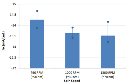
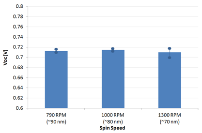
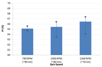
Reference device were made on batch M211 to assess the effect of PTB7:PC70BM active layer thickness on OPV efficiency using an inverted architecture with the below structure. These consisted of the below structure and were fabricated under inert atmosphere (glovebox) before encapsulation and measurement under ambient conditions.
Glass / ITO (100 nm) / PFN (6.5 nm) / PTB7:PC70BM (1:1.5) / MoOx (15 nm) / Al (100 nm)
For generic details please see the general fabrication guide and video. For specific details please see the below condensed fabrication report which details the optical modelling and optimisation of the multilayer stack.
Previously it has been shown that PFN of around 6.5 nm gives optimum performance [1-3,P021] while modelling has shown that an Al back cathode gives higher performance than Ag when used with MoOx [4].
The PTB7:PC70BM solution was made in chlorobenzene at 25 mg/ml before being diluted with 3% diiodooctane (DIO) to promote the correct morphology.
Active layer thicknesses of 75 nm, 90 nm and 105 nm were chosen corresponding to the lower, middle and upper end of the "thin film" absorption peak of a typical stack as predicted by optical modelling [1]. For each of these thickness a total of four substrates was produced, each with 4 pixels and the data presented below represents a non-subjective (no human intervention) analysis of the best 75% of pixels by PCE (12 pixels for each condition).
An additional two substrates were also prepared with a methanol wash to help remove the DIO as has been reported in the literature to help improve performance[5].
Overall, the maximum efficiency of 7.2% average PCE (7.4% maximum) was found at 75 nm film thickness.


Note 1: Dektak Thickness calibration
We normally calibrate thin films by use of a Dektak surface profiler, however the use of DIO results in an enhanced level of uncertainty in the film as the DIO will take several hours to fully dry under normal conditions and is likely to undergo some slight further shrinkage when placed in vacuum. The DIO can also be removed by baking the substrate on the hotplate at 80°C for about 10 mins which can be useful for doing quick measurements but also drives excess phase separation between the polymer and PCBM making it unsuitable for device work.
Note 2: Effect of epoxy
Due to the very high solubility of the PTB7 it was noted during fabrication that the film changed colour when in contact with the Ossila encapsulation epoxy in liquid form for extended periods indicating that there was some miscibility. Inspection of the active areas underneath the top cathode indicated that the epoxy had not seeped into the active area before curing and device metrics indicate that this did not appear to affect performance. However, we would recommend minimising contact time between the epoxy and PTB7 films before UV curing.
Fabrication
Substrates and cleaning
- Pixelated Cathode ITO glass substrates (S171)
- 5 mins sonication in hot Hellmanex III (1 ml in beaker)
- 2x boiling water dump rinses
- 5 mins sonication in warm IPA
- 2x dump rinses
- 5 mins sonication in hot NaOH
- Dump rinse in boiling water
- Dump rinse in water
- Stored in DI water overnight and until use
PFN Solution
- Acetic acid dissolved 1:9 in methanol to make stock solution
- 2 μl/ml (0.2 v%) solution of acetic solution in methanol made by diluting the stock solution by 50 times in methanol
- PFN dissolved in the 0.2 v.% acetic acid solution at 2 mg/ml
- Stirred for 30 mins
- Filtered through 0.45 µm PES filter
PFN Test Films
- PFN Test film initially spun at 500 rpm and gave 20 nm
- Second test film spun at 1000 rpm and gave 16 nm
- Thickness was extrapolated to 6.5 nm at 6000 rpm
Active Layer Solution
- Fresh stock solutions of PTB7 (M211) made on at 10 mg/ml in chlorobenzene (CB) and dissolved with stir bar for 1 hour
- Mixed 1:1.5 with dry Ossila 99% PC70BM to make overall concentration of 25 mg/ml and dissolved with stir bar for 1 hour
- Old stock solution of 1,8-Diiodooctane mixed 1:1 with CB to make measuring out small quantities easier
- DIO/CB mixture added to solution to give overall DIO amount of 3%
Active Layer Test Films
- Test film spun at 1000 rpm for 2 mins using unfiltered solution and dried using methanol before Dektak
- 1000 rpm gave approximately 85 nm
Active layers
- Devices spun using 30 μl dynamic dispense (20 μl gave only moderate wetting/coverage)
- Non methanol devices spun for 2 mins
- Methanol devices spun for 30 seconds, then coated with 50 μl methanol by static dispense then spun at 2000 rpm for 30 seconds.
- Cathode wiped with CB
- Vacuum dried in glovebox antichamber for 20 mins
Evaporation
Left in chamber over the weekend and evaporated with the below parameters.
- 15 nm MoOx at 0.2 Å/s
- 100 nm Al at 1.5 Å/s
- Deposition pressure
Encapsulation
- As standard using Ossila encapsulation epoxy, 30 mins UV in MEGA LV101
Measurements
- JV sweeps taken with Keithley 237 source-meter
- Illumination by Newport Oriel 9225-1000 solar simulator with 100 mW/cm2 AM1.5 output
- NREL certified silicon reference cell used to calibrate
- Lamp current: 7.8 A
- Solar output at start of testing: 1.00 suns at 25°C
- Solar output at end of testing: 1.00 suns at 25°C
- Air cooled substrates
- Room temperature at start of testing: 25°C
- Room temperature at end of testing: 25°C
- Calibrated aperture mask of size 0.256 mm2
Standard (Non-inverted) Reference Devices
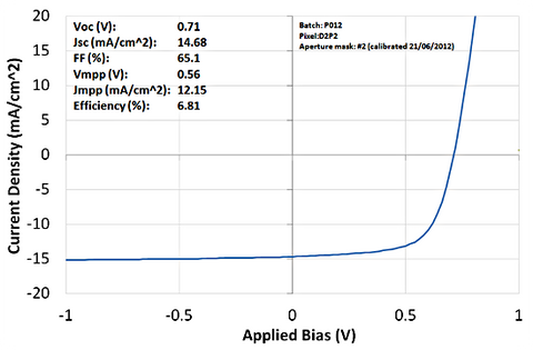
Reference device were made on batch M211 using a standardised architecture for comparative measurements using Ossila standard substrates and materials. These consisted of the below structure and were fabricated under inert atmosphere (glovebox) before encapsulation and measurement under ambient conditions.
Glass / ITO (100 nm) / PEDOT:PSS (30 nm) / PTB7:PC70BM (variable) / Ca (2.5 nm) / Al (100 nm)
For generic details please see the fabrication guide and video. For specific details please see the below condensed fabrication report and also Watters et al. [3] which details the optical modelling and optimisation of the multilayer stack.
For this standard reference architecture an average PCE of 6.6% was achieved for the optimised thickness with a peak efficiency of 6.8%. Note that no other optimisation was performed (blend ratio, DIO concentration, drying conditions etc) and so further small improvements may be obtained by varying these conditions and significant improvements obtained by using alternative interface materials [1,2].

Note 1: Dektak Thickness calibration
We normally calibrate thin films by use of a Dektak surface profiler, however the use of DIO results in an enhanced level of uncertainty in the film as the DIO will take several hours to fully dry under normal conditions and is likely to undergo some slight further shrinkage when placed in vacuum. The DIO can also be removed by baking the substrate on the hotplate at 80°C for about 10 mins which can be useful for doing quick measurements but also drives excess phase separation between the polymer and PCBM making it unsuitable for device work.
Note 2: Effect of epoxy
Due to the very high solubility of the PTB7 it was noted during fabrication that the film changed colour when in contact with the EE1 encapsulation epoxy in liquid form for extended periods indicating that there was some miscibility. Inspection of the active areas underneath the top cathode indicated that the epoxy had not seeped into the active area before curing and device metrics indicate that this did not appear to affect performance. However, we would recommend minimising contact time between the epoxy and PTB7 films before UV curing.
Fabrication
Substrates and cleaning
- Pixelated Cathode substrates (S171)
- 5 mins sonication in hot Hellmanex (1 ml in beaker)
- 2x boiling water dump rinses
- 5 mins sonication in warm IPA
- 2x dump rinses
- 5 mins sonication in hot NaOH
- Dump rinse in boiling water
- Dump rinse in water
- Stored in DI water overnight and until use
PEDOT:PSS layer preparation
- Clevios AI 4083
- Filtered into vial using 0.45 μm PES filter
- Spun 6000 rpm for 30 seconds (30 nm)
- Dynamic dispense of 20 μl using pipettor
- IPA cathode strip wipe and labelled
- Put straight onto hotplate at 160°C as soon as cathode wiped and labelled
- Transferred to glovebox when all samples spun.
- Baked in glovebox at 150°C for 1 hour
Active layer Solution Preparation
- Fresh stock solutions of PTB7 at 10 mg/ml in CB and shaken to dissolve
- Mixed 1:1.5 with dry Ossila 99% C70 PCBM to make overall concentration of 25 mg/ml
- 1,8-Diiodooctane mixed 1:1 with CB to make measuring out small quantities easier
- DIO/CB mixture added to solution to give overall DIO amount of 3%
Active layer spin casting
- Devices spun for 2 mins using 25 μl dynamic dispense
- Cathode wiped with chlorobenzene
- Left to dry in glovebox for 2 hours but colour indicated they were still slightly wet
- Dried in vacuum in glovebox antichamber for 10 mins to remove DIO
Evaporation
Left in chamber over the weekend and evaporated with the below parameters.
| Material | Ca |
| Base pressure | 8.0 E-8 mbar |
| Dep start pressure | 1.7 E-7 mbar |
| Max pressure | 2.7 E-7 mbar |
| Thickness | 2.5 nm |
| Rate | 0.2 Å/s |
| Material | Al |
| Base pressure | 7.0 E-8 mbar |
| Dep start pressure | 6.0 E-7 mbar |
| Max pressure | 7.0 E-7 mbar |
| Thickness | 100 nm |
| Rate | 1.0 Å/s |
Encapsulation
- As standard using Ossila encapsulation epoxy, 30 mins UV in MEGA LV101
Measurements
- JV sweeps taken with Keithley 237 source-meter
- Illumination by Newport Oriel 9225-1000 solar simulator with 100 mW/cm2 AM1.5 output
- NREL certified silicon reference cell used to calibrate
- Lamp current: 7.8 A
- Solar output at start of testing: 0.99 suns at 25°C
- Solar output at end of testing: 1.00 suns at 25°C
- Air cooled substrates
- Room temperature at start of testing: 21°C
- Room temperature at end of testing: 21°C
- Calibrated aperture mask of size 0.256 mm2
MSDS Documentation
 PTB7 MSDS sheet
Pricing
| Batch | Quantity | Price |
| M215 | 100 mg | £297.00 |
| M216 | 100 mg | £297.00 |
| M216 | 250 mg | £594.00 |
| M216 | 500 mg | £1010.00 |
| M216 | 1 g | £1820.00 |
Batch Information
| Batch No. | Mw | PDI | Stock Info |
| M211 | 18,000 | 1.75 | Discontinued |
| M212 | > 40,000 | 2.0 | Discontinued |
| M213 | 85,000 | 2.0 | Discontinued |
| M214* | 322,236 | 4.12 | Discontinued |
| M215 | 125,821 | 2.02 | Low in stock |
| M216 | 78,852 | 2.62 | In Stock |
Literature and References
- Enhanced power-conversion efficiency in polymer solar cells using an inverted device structure Zhicai He et al., Nature Photonics, V 6, p591–595 (2012).
- Simultaneous Enhancement of Open-Circuit Voltage, Short-Circuit Current Density, and Fill Factor in Polymer Solar Cells Zhicai He et al., Advanced Materials, V 23, p4636–4643 (2011).
- Optimising the efficiency of carbazole co-polymer solar-cells by control over the metal cathode electrode Darren C. Watters et al., Organic Electronics, V 13, p1401–1408 (2012)
- Designing ternary blend bulk heterojunction solar cells with reduced carrier recombination and a fill factor of 77%, N. Gasparini et al, Nat. Energy, 16118 (2016); doi:10.1038/nenergy.2016.118 (Ossila PTB7 was featured in this paper).
To the best of our knowledge the technical information provided here is accurate. However, Ossila assume no liability for the accuracy of this information. The values provided here are typical at the time of manufacture and may vary over time and from batch to batch.
ebiomall.com


>
>
>
>
>
>
>
>
>
>
>
>


