We are pleased to announce that the price of this product has recently been reduced from £425 to £199. We are thankful to our customers for their increased demand and support - you have allowed us to scale-up production and pass these savings back to you!
*If you have purchased this item between 1st Jan 2019 and 14th April 2019, please contact us at info@ossila.com.
Pre-patterned ITO substrates for OPV/OLED testing. Use with our cathode deposition mask (E341) to create individual pixels.
Datasheet
Substrate size
20 mm x 15 mm
Thickness
1.1 mm
Pixel dimensions (with cathode)
3 mm x 1.5 mm (4.5 mm2)
Glass type
Polished soda lime, float glass
Substrate coating
Fully oxidized ITO
ITO thickness
100 nm
ITO resistance
20 Ω / square
Glass roughness
<1 nm rms By AFM
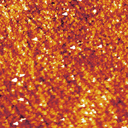
ITO roughness
1.8 nm RMS (By AFM)
10 µm x 10 µm AFM scan with Z-scale of ±5 nm.
AFM of glass surface (1 µm x 1 µm x 3.5 nm). Courtesy of Richard T Grant.
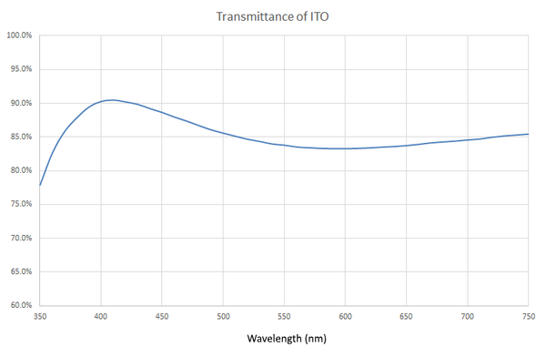
Transmittance of ITO substrates
To the best of our knowledge, the information provided here is accurate. However, Ossila assume no liability for the accuracy of this information. The values provided here are typical at the time of manufacture and may vary over time and from batch to batch.